What is the reason why "Au Stud Bump" is increasing its presence in the flow of IoT? Ask Hakodate Electronics, the top runner of Au stud bump processing
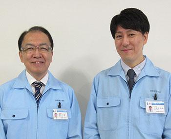
Mr. Masaaki Kurosu, Representative Director, Hakodate Electronics Co., Ltd. Mr. Hideki Kubota, Manager, Engineering Section
Au stud bumps are so-called "gold protrusion electrodes" that connect the terminals of the IC chip circuit to the circuit of the board. In addition to Au stud bumps, there are several types of stud bumps, such as solder stud bumps. Among them, Au stud bumps are used for products that require high reliability and accuracy. This time, we will talk to Hakodate Electronics Co., Ltd. in Hakodate City, Hokkaido, which is engaged in the manufacturing and inspection of electronic parts and other post-processes of semiconductors, about the reason why Au Stud Bump is increasing its presence in the flow of IoT. rice field.
As IoT and AI evolve, the needs for semiconductors in various industries and fields are expected to increase in the future. Under such circumstances, a processing method called "Au stud bump bonding", which is indispensable for manufacturing fine and highly accurate IC chips, is increasing its presence. What is an Au stud bump in the first place and what is amazing? We interviewed Mr. Masaaki Kurosu, CEO of Hakodate Electronics Co., Ltd., a top runner of Au stud bump processing, and Mr. Hideki Kubota, Manager of the Technology Division.
Strong in fine and highly accurate Au stud bump processing
Hakodate Electronics is a company based in Hakodate City, Hokkaido, which is engaged in the manufacturing of semiconductor post-processes such as the manufacture and inspection of electronic components. In addition to wafer level Au stud bump bonding, we also carry out IC chip dicing, LED chip probe testing, and sorting business. In particular, the company's strength is fine and highly accurate Au stud bump processing, which can be used to process individual IC chips. We have a good reputation for "speedy", "accurate", "reasonable" and "stable quality" while working on a wide range of products from prototypes to mass-produced products. Since the number of companies with these strengths is limited, we have received many inquiries from well-known major companies, and we have also worked on the world's most accurate semiconductor sensors and watches.


What is Au stud bump?
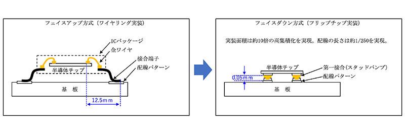
Au stud bumps are so-called "gold protrusion electrodes". Conventionally, gold wire has been used to connect the terminal of the circuit of the IC chip and the circuit of the board. However, with the trend toward lighter, thinner, shorter and smaller electronic devices, it has become necessary to make gold wires, which are several millimeters long, even shorter, and the result is flip-chip mounting. Instead of using a gold wire, attach a gold protrusion electrode to the connection terminal of the IC chip circuit, turn it over, and connect it directly to the circuit.
Used for high precision products
In addition to Au stud bumps, there are several types of stud bumps, such as solder stud bumps. Among them, Au stud bumps are used for products that require high reliability and accuracy. "For example, for products that do not require such high precision, the current trend is to use inexpensive solder stud bumps. However, since it is necessary to connect 100 pads or more, it naturally takes time to process. On the other hand, gold is expensive, but its conductivity is very good and it does not corrode. Due to these characteristics, it is customary to use Au stud bumps for products that require high quality. Also, Au stud bumps are chips. There are few terminals in the connection circuit, and it takes less than 40 pads, so it does not take much processing time. Each stud bump has its own characteristics. "(Mr. Kurosu)
Tendency to become finer
Au stud bumps are characterized by the need for finer processing with the times, but how much finer processing is specifically required in the field? "The first Au stud bump I started making was about 100 μm, which is about the size of a human hair. However, recently, there have been cases where diameters up to 50 μm (0.05 mm) are required. For example, it is indispensable for smartphone parts. When the crystal oscillator is made smaller, the IC chip also needs to be made smaller. As a result of continuing to take on the challenge in anticipation of the need to make the diameter of the Au stud bump smaller, we have been able to handle up to 25 μm over 20 years. Since it is a technology that can be used for small chip of sensor system, there should be a tendency that fineness will continue to be required in the trend of IoT etc. "(Mr. Kurosu)
Few companies can handle mass production
Au stud bump processing is also characterized by the fact that few companies can handle mass production. "Au stud bumps are not something you can do by simply buying a device. There are various setting conditions for the device, and you need to make full use of them. Anyone can do it. The difficult thing is that each customer has detailed specifications. To meet the different conditions for each customer such as shape, height, thickness, and position accuracy, many years of experience and know-how are required. "I say" (Mr. Kurosu) "There are other companies that can handle projects that are OK if you make a prototype. However, when dealing with mass-produced products, only those with high quality quickly, accurately, and stably are reasonably priced. In addition to technical capabilities, quality control know-how is indispensable in order to continue to provide to us. In that respect, we have experience and know-how cultivated over 20 years. The defect rate of mass-produced products is about 50ppm to 300ppm. However, this cannot be easily imitated by other companies. "(Mr. Kubota) Au stud bump bonding equipment is expensive, costing about 15 million yen per unit. While the number of companies that can install multiple devices is limited, Hakodate Electronics owns 24 devices. We are proud of the number of units we own, which is one of the best in Japan, which is also the reason why we can handle a wide range from prototypes to mass production.
Achievements that have supported "the world's highest peak" manufacturing with Au stud bumps
Fine and high-precision Au stud bump processing by Hakodate Electronics has been adopted in various manufacturing of so-called first-class companies. For example, semiconductor sensors and watches that boast the highest accuracy in the world. "There was a customer request for the IC chip used for semiconductor sensors to have a uniform height. The tip of the stud bump is like a protrusion, so hit all the tips of the stud bump once made. This was our first attempt to make the height uniform. However, once we decided on the materials and conditions, we were able to quickly clear the manufacturing process with our know-how. The difficulty was quality control. However, when the tip of the stud bump is crushed flat, if foreign matter or dirt adheres to it, the shape will change, so it took time for quality control after making it. When I came to our company for such reasons, not only the technical aspect but also the management aspect was evaluated, which led to mass production. "(Mr. Kubota) In addition, the company manufactures crystal oscillators that are indispensable for mobile phones and smartphones. We have a large company as a customer. We have a track record of exclusively delivering all of the Au stud bumps used by our customers, which is also due to the company's technical and quality control aspects. "In fiscal 2016, we made 400 million IC chips for crystal oscillators in one year. In fiscal 2017, 1.4 billion smartphones were manufactured worldwide, so less than 30% of the products we worked on were IC chips. It is a calculation that is included. In any case, we have heard from customers that there are no complaints from end users regarding our products. "(Mr. Kurosu)
I want to continue making electronic components that are at the cutting edge of the times
As IoT and AI evolve, the needs for IC chips and electronic circuits will continue to grow in industries and fields that were previously unnecessary. What kind of future is Hakodate Electronics looking at? "We have been working on cutting-edge components for a long time, but we want to continue to be in that position. In the age of digital transformation, which makes people's lives better, we are smaller. There will be more robot-related goods and services that we have to do. I think Au stud bump processing will be more useful, so I would like to open up new markets, including fields that I have never had a connection with before. " Mr. Kurosu) If you have any problems or inquiries regarding fine and highly accurate electronic components, from prototypes to mass-produced products, please feel free to contact Hakodate Electronics.
Hakodate Electronics Co., Ltd. Founded in 1982. Engaged in manufacturing of semiconductor post-processes such as manufacturing and inspection of electronic parts. Its strength is Au stud bump bonding, which is particularly fine and highly accurate, and it boasts one of the largest number of units in Japan. We have a track record of working on various products from prototypes to mass-produced products.Hakodate Electronics Co., Ltd. Inquiries