Performance comparison of IGBT PIM and SiC MOSFET PIM in solar inverter
Figure 1: Comparison of voltage drops between IGBT PIM and SiC MOSFET PIM at 125 ° C
The dynamic loss is frequency dependent, and when comparing the IGBT and SiC MOSFET in Figure 1 with a switching operation of about 20A to 30A at the same low frequency (eg 16kHz), the conduction loss is similar but the dynamic loss is Varies. Figure 2 shows the two causes of switching loss: turn-on energy Eon and turn-off energy Eoff, respectively. There is a cross point here as well, but Eon is almost the same, both device types are about 1/4 of the conduction loss, and the IGBT is a little lower, but the absolute value is not large. However, in IGBTs, as the collector voltage rises, a "tail" current (a minority carrier that must be discharged from the device's N-drift region at turnoff) flows, resulting in much larger and transient power loss. increase. Figure 2 shows that there is a 10-fold difference in Eoff between both device types.
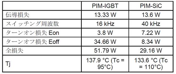
Table 1 summarizes the differences when operating a practical PV boost converter with an input of 500V / 25A and an output of 800 VDC at 16kHz and a case temperature of 95 ° C. Overall, SiC is clearly more power-saving, has a total loss of about one-third that of the IGBT circuit, and is more reliable due to its lower junction temperature.
SiC MOSFET score at higher frequencies
In addition to energy savings, the benefits of increased efficiency with SiC include reduced heatsink size and cost, reduced temperature rise for the same heatsink, or improved power throughput for the same heatsink and temperature rise. All of these are valuable benefits, but it is worth investigating the situation when taking advantage of the high frequency performance of SiC. Table 2 compares a SiC MOSFET with a switching frequency of 40 kHz and an IGBT of 16 kHz.

SiC devices have higher junction temperatures, but because they are WBG devices, they support an operating temperature that is 25 ° C higher than silicon. The results of the SiC MOSFET show that it is more efficient than the IGBT, the loss is reduced by about half, and all the above-mentioned advantages are greatly demonstrated. However, the increased frequency can reduce the value and size of the boost inductor by about one-third, resulting in cost, size, and weight savings. In addition, EMI filtering at fundamental frequencies and low harmonics can be reduced, leading to further cost savings. However, SiC MOSFETs have high edge rates, so high frequency filtering must be carefully considered to meet emission standards.
Loss is not the only difference between IGBTs and SiC MOSFETs. For example, MOSFETs have body diodes, but IGBTs do not. This is useful in transformation stages where the switch requires reverse or "third quadrant" conduction. The body diode of the SiC MOSFET can take advantage of the relatively large forward voltage drop. When using the IGBT in this way, an extra parallel diode needs to be added.
Therefore, there are significant system advantages when using SiC at higher frequencies, which can be balanced in that it far outweighs the difference in PIM unit price between both technologies. As new generations of devices emerge and the on-resistance of SiC MOSFETs decreases, the benefit crosspoints are expanded to higher output levels for a wider range of applications than ever before.
Careful design is required to bring out the performance of SiC
Although the gate drives of IGBTs and SiC MOSFETs look similar at first glance, the on-drive of SiC devices is more important to minimize conduction loss and is the absolute maximum voltage practically possible. Must be close to 25V. Therefore, 20V is often used to ensure some safety margin. Both device types are nominally turned off with a 0V gate drive, but are often driven negative by a few V. This reduces Eoff, reduces gate-source ringing during turnoff, and helps prevent "phantom turn-on" due to spikes caused by source or emitter inductance common to gate drive loops.
The device's "mirror" capacitance also tends to pseudo-turn on the device when the drain or collector voltage edge rate (dV / dt) is high. Again, a negative gate drive can help avoid the problem. Figure 3 shows the effect.
Since SiC MOSFETs have much higher dV / dt and di / dt than IGBTs, practical circuits must use carefully decoupled high frequency layout techniques to avoid unreliable operation and excessive EMI. Must be. The driver should be located close to the SiC MOSFET PIM and a "Kelvin" connection to a possible MOSFET source should be used as the driver return to avoid common inductance.
Accurate measurement of the dynamic performance of a SiC MOSFET PIM is difficult due to the high edge rate, so it is generally necessary to use equipment with a bandwidth of 300MHz and high frequency measurement techniques. The voltage probe is connected with a minimal ground loop and the current is monitored by a high performance sensor such as a Rogoski coil.
summary
Switching from IGBTs to SiC MOSFETs is a system benefit in terms of increased power levels, and PIM is an easy solution. However, those familiar with the use of IGBTs should be aware that simply replacing them will not give good results. Gate drive placement, layout, and EMI filtering should be reassessed for optimal performance.
