Think about signal integrity in high -speed digital circuits
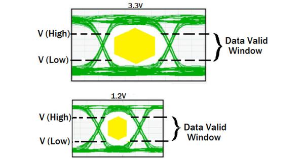
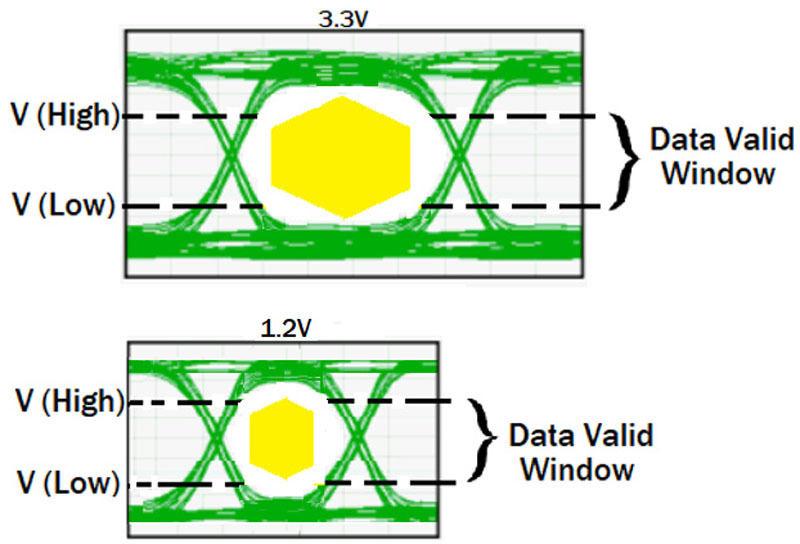
Fig. 1 The impact of frequency increase and voltage decrease on the eye pattern
In specific high -frequency design, if other design issues such as signal attenuation, reflection, impedance consistency, jitter are added, it will be difficult for the receiver to accurately interpret information due to signal loss, causing an error occurrence.It is clear that the opportunity will increase.
Sampling by clock in the data stream
On the receiver side, the data is sampled in the standard clock edge.The larger the eye opening, the easier it is to set the sampling clock in the center of the specific bit and sample the data.When the amplitude, reflection, jitter, etc. occur, the eye diagram becomes smaller, the data effective window and the effective bit time are substantially narrow, causing errors on the receiving side.
Here, we will consider cases where channel or interconnected connections need to be treated as a transmission line, and focus on the main reasons for which transmission loss occurs in systems such as smartphones and tablets.
High frequency and transmission line
"Low -frequency design" is when the wavelength is much longer than the wiring length, and the electrical resistance between PCB traces and interconnection does not depend on the frequency.Therefore, the impact of the transmission line can be ignored.
On the other hand, in "high -frequency design", the wavelength is much shorter than the wiring length, and all the physical characteristics of the trace and the dimensions of interconnection are controlled.As a result, a transmission line with a series of electrical characteristics can be secured for specific applications.
A high -frequency movement that needs to be treated as a single transmission line is when the trace length is about 1/10 or higher than the wavelength of the frequency used.
At this point, it is necessary to model traces using multiple intensive elements.It is also necessary to take into account all elements that depend on the frequency, including parasitic capacity and parasitic inductance, and the effects of those elements on signal attenuation.
Another way to determine the frequency that needs to be treated as a transmission line is to consider the signal rising time (TR).
In most of the NM process nodes, high data rates signals are steep/down, and it is necessary to handle channels or interconnection as transmission lines.When these signals flow via a channel, their bandwidth and propagation delay depend on the rising time of the signal.
Propagation speed
Electrical signals are electromagnetic waves, and the propagation speed depends on the dielectric ratio of substances surrounding the surroundings.The formula of the propagation speed is as follows.
自由空間(誘電率1)内を伝達される無損失送信の波形速度は約3×10⁸m/sですが、誘電率が4の伝送ラインを伝達される波形速度はこれとは異なり、およそ半分つまり1.5×108m/sに低下します。
Differences in the waveform speed transmitted in the free space and the PCB have a delay time of propagation delay (TD).This value depends on the medium used for propagation and the distance that the signal is transmitted.
TD (propagation delay) = travel distance/VP (propagation speed)
Then, on the other hand, what if a signal (clock) propagates an external layer and another signal (data) propagates internal layers in a situation where there is an empty space and the other side exists on the other side.。
In many designs, high -frequency signals need to pass through an interconnection or flat cable as part of the route.As a result, delays and shifts occur in both the amplitude and timing of the waveform.Due to a decrease in signal speed, a cross -talk, or a slipping of the timing caused by the energy absorption by dielectric substances, or the accompanying loss, both the timing and the amplitude may have a amplitude called "jitter".
In this situation, the designer needs to match the flight time (time required for movement) between the series of signals.The data signal that flows internal layers has a decrease in propagation speed, so it is necessary to shorten the length of the data signal in order to consistent with the clock signal flight time.
Epidemic effect
Assuming a part of the C1 conductor and flowing current I (t) there, a magnetic flux that is proportional to the current flowing through the conductor is generated based on the law of the ampel.

If one conductor exists alone and no other conductor is nearby, a whirlpool current that circulates in the conductor C1 in the opposite direction of magnetic field B1 due to a magnetic flux line (B1).
As the frequency increases, the epidermis effects cause the area where the current flows in the cross -sectional area of the conductor, increasing the substantial electric resistance, increasing the response.
Transmission line and characteristic impedance ZO
The voltage and current on the transmission line flow together, and these are represented as a function of both position (x) and time (t).The characteristic impedance of the transmission line (ZO) is a resistance that depends on the frequency, and can be represented by the voltage waveform to the propagated current waveform.
When the waveform of voltage V (x, t) and current I (x, t) propagates together and reaches the terminal impedance, V (x, t)/I (x, t) ends with ohm's law.It must be equal to impedance (ZL).
When a high -frequency signal is propagated via a multiple path in one PCB, the impedance changes when passing through the beer or when changing the route from a layer to another layer.
Focusing on a specific PCB will show that there are many layers, traces, beer, and connections that have changed at any point.In addition, there are parasitic components that support self -contained capacity, mutual static capacity, and self -inductance and mutual inductance.
Here, let's introduce some concentrated elements that exist in any system, such as parasitic inductance, electrostatic capacity, AC skin resistance, and DC resistance.
For example, what kind of changes the parasitic capacity (CDX) may cause the current distribution, and what is the characteristic impedance of the transmission line and the ZO (ratio of the propagation voltage to the propagation current) due to a change in current distribution.You can check if it will change.
If the amplitude of the inflow signal decreases due to the skin effect, the voltage between the parasitic inductance may reduce the rising time of the voltage between the loads and the falling time, which affects the quality of the signal and the deterioration of the signal. There is a possibility.
Voltage reflective coefficient
When a high -frequency signal is propagated via a different route, the impedance changes when passing through the beer or when changing the route from a layer to another layer.
If these parasites are controlled and the transmission line is properly terminated, the signal can be propagated with minimal distortion.
If the terminal impedance (ZL) is not equal to the line characteristic impedance (ZO), there will be a pair of the reflective voltage waveform and the reflective current waveform, but these reflective signals interfere with the source signal and distorted.Causes.
If the load terminal impedance (ZL) is equal to the characteristic impedance (Zo) of the transmission line, the voltage reflective coefficient is equal to 0.This value means that all incident waves are absorbed by the consistent load end.
When both voltage waveforms and current waveforms are propagated, and reach the terminal impedance, the total of V/I's reflected waves must be equal to the terminal impedance (ZL).
Importance inconsistency and reflection
Use a 50Ω transmission line to consider the case where it ends with a 150Ω terminal impedance or over -damping circuit.To make it easier, set the battery impedance to 0, which always generates reflective waves toward the load.It also sets a delay time (TD = distance/VP) that requires this waveform to move a certain distance.Close the switch here and observe what will happen with the load.
Continuous reflection waves are generated in two directions between the source and the terminal impedance, and these reflected waves interfere with the source signal, creating linging on the signal line.
Calculating the reflection coefficient on both the terminal and source, it will determine the size of the incident wave that will eventually reach the terminal side and the size of the reflective wave bouncing back toward the source.
The over -shutring ring shown in Fig. 14 has reached a high voltage, giving a large radiation, excessive stress, and may generate substantially further cross -talk between adjacent traces.
On the other hand, both under shots due to linging or voltage drops on the transient response period may increase bit error rate.
System that uses lid driver and not used
For example, USB 3 with data rate 10Gbps.In the case of a mobile application that uses 1 Gen 2, there is a total loss of the total loss in DB units, including channel losses in all interconnection.Loss tolerates include the loss generated in all routes from silicon to connectors, such as packages of silicon products, PCB traces, beer, flat cables, common mode filters, connectors, etc.
To maintain good signal quality with the USB Type-C Gen 2 system without restrictions on the size or device position of the PCB, the Ridoribar is the most cost-effective solution.When considering systems such as smartphones and tablets, high -frequency digital signals may flow through the application processor's package and pin via PCB trace, beer, connector, flat cable, and USB connector.As a result, the high data rate signal may have already deteriorated before flowing through a 1m cable.
When the signal flows via the channel, the signal amplitude may decline, depending on the length of the channel, this attenuation may increase, and if the data rate is high, the signal integrity problem may occur.
Using a ridoriver as a signal conditioning device can recover signals that have increased the loss on a specific channel and amplify the output of the signal after recovery.This makes it possible to transmit the signal over a longer distance, enlarging the eye opening and reducing bit errors.
Using a programmable differential output voltage lid driver ensures a drive strength suitable for line impedance and tracing lengths, homogenizing signals, and solving the signal integrity problem.If the differential output voltage is increased on the driver side, the signal on the receiving side will be improved, but it should be noted that noise and jitter will increase.
summary
To maintain a tolerant signal integrity, it is necessary to consider the effects of epidermal effects, integrated ends, reflections, beer, crosstalk, coupling, and the effects of the signal attenuation.
If the trace length is about 1/10 or more of the signal wavelength, all interconnection must be considered a single transmission line.
The factors that affect the signal integrity are channel losses and signal reflections, such as the reflection of these, such as the data flows from the processor to the PCB, beer, and flat cable, or the reflection of the path in the opposite direction.It is an inconsistency of impedance that occurs when passing.
In order to prevent reflection and realize the maximum power transmission, it is important to establish an interface that maintains impedance in the entire signal path.No impedance inconsistency causes reflections on the line, in which case jitter may occur and the signal quality may deteriorate.
If you do not use redrawers, it will be very difficult or almost impossible to pass electrical characteristics and protocol -compliant tests in data rates that exceed 10Gbps.When testing both short and long -distance channels, if you do not use a ridoriver, it is unlikely that interoperability can be realized between various devices, and can be used at specific signals that use high data rates.The distance of the general transmission channel may be limited.
